The LUX1-16K™ chip measures 2.7 mm x 2.4 mm and uses small chip scale packaging with Cu bumps.
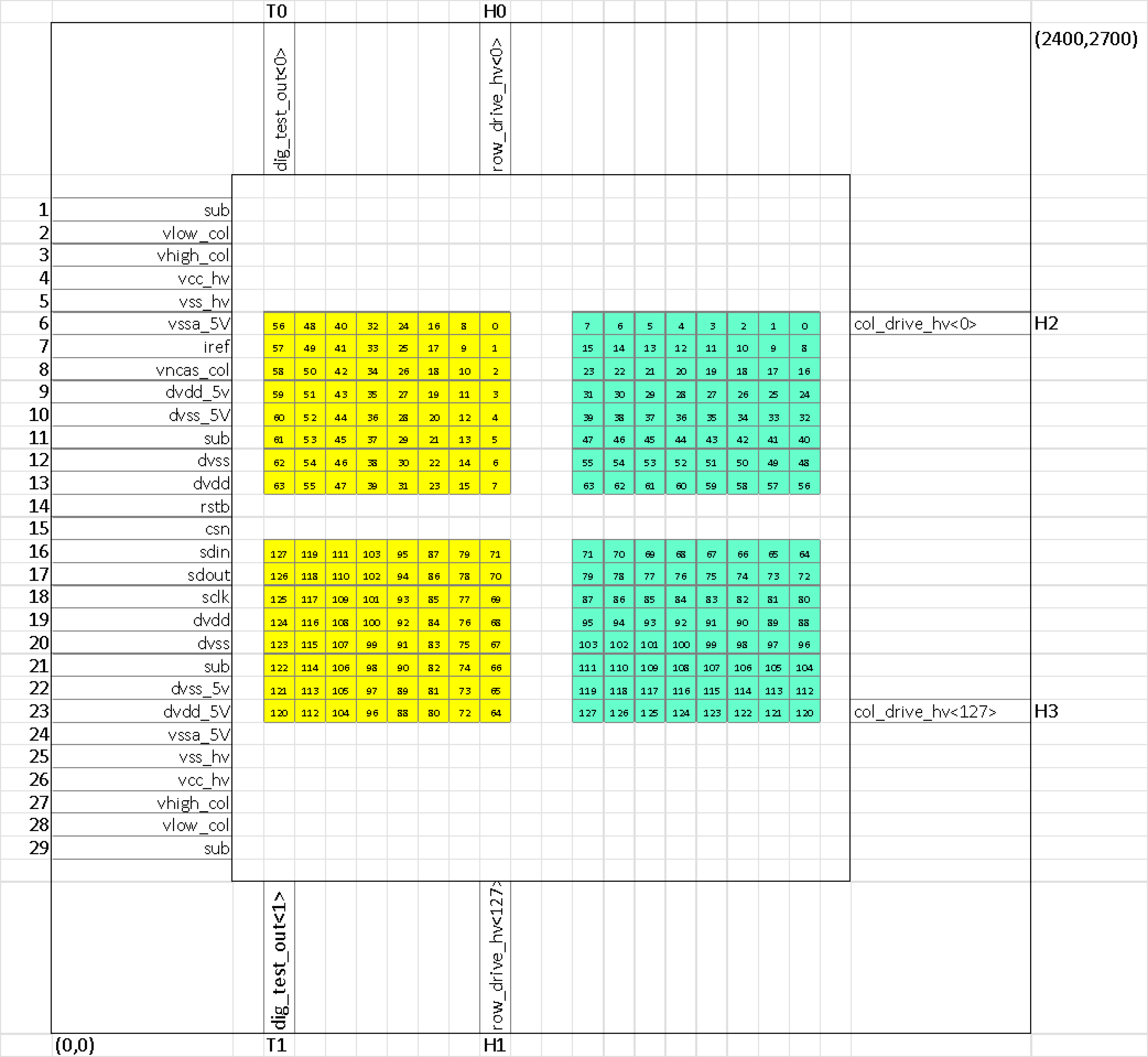
Bump Locations
| No. | Pad Name | Location | Center of wire bond pad (X,Y) in µm |
|---|---|---|---|
| 1 | sub | LEFT | 50, 2470 |
| 2 | vlow_col | LEFT | 50, 2390 |
| 3 | vhigh_col | LEFT | 50, 2310 |
| 4 | vcc_hv | LEFT | 50, 2230 |
| 5 | vss_hv | LEFT | 50, 2150 |
| 6 | vssa_5V | LEFT | 50, 2070 |
| 7 | iref | LEFT | 50, 1990 |
| 8 | vncas_col | LEFT | 50, 1910 |
| 9 | dvdd_5v | LEFT | 50, 1830 |
| 10 | dvss_5V | LEFT | 50, 1750 |
| 11 | sub | LEFT | 50, 1670 |
| 12 | dvss | LEFT | 50, 1590 |
| 13 | dvdd | LEFT | 50, 1510 |
| 14 | rstb | LEFT | 50, 1430 |
| 15 | csn | LEFT | 50, 1350 |
| 16 | sdin | LEFT | 50, 1270 |
| 17 | sdout | LEFT | 50, 1190 |
| 18 | sclk | LEFT | 50, 1110 |
| 19 | dvdd | LEFT | 50, 1030 |
| 20 | dvss | LEFT | 50, 950 |
| 21 | sub | LEFT | 50, 870 |
| 22 | dvss_5v | LEFT | 50, 790 |
| 23 | dvdd_5V | LEFT | 50, 710 |
| 24 | vssa_5V | LEFT | 50, 630 |
| 25 | vss_hv | LEFT | 50, 550 |
| 26 | vcc_hv | LEFT | 50, 470 |
| 27 | vhigh_col | LEFT | 50, 390 |
| 28 | vlow_col | LEFT | 50, 310 |
| 29 | sub | LEFT | 50, 230 |
The Row Drive and Column Drive output bumps are located in the core of the chip. The LEFT arrays are assigned to Row Drive outputs and the RIGHT arrays are assigned Column Drive outputs. The shape and locations of the Row Drive and Column Drive bumps are provided in the mechanical drawing of the LUX1-16K chip, provided under NDA.