Creating wafers with the Two Layer TFE process will result in a chip with up to 9 layers: GaN LED, three polyimide layers, three metal layers, Cu and Sn plating, and TiN electrodes. Two Layer TFE products are shipped on substrate.

| Layer name | Thickness (µm) | Purpose |
|---|---|---|
| GaN LED | 5.5 | This layer adds µLEDs with a wavelength of 530 nm. |
| Polyimide 1 | 5 | This layer forms the base of the device. |
| Metal 1 | 0.26 | This layer is ideal for routing traces and defining electrode or LED sites. |
| Polyimide 2 | 2.5 | This layer insulates the routing traces. |
| Metal 2 | 0.26 | This layer is ideal for routing traces and defining electrode or LED sites. |
| Polyimide 3 | 2.5 | This layer insulates surface mounted components from routed traces. |
| Top metal | 0.12 | This layer is ideal for remetallizing electrode sites and connection pads. |
| TiN | 0.5 | This layer is used for electrode material. |
| Plating | 17 | This layer is used for die attachment areas. |
Examples
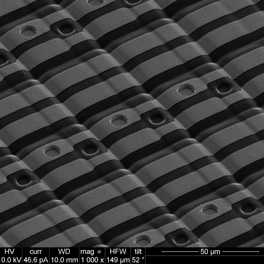 | 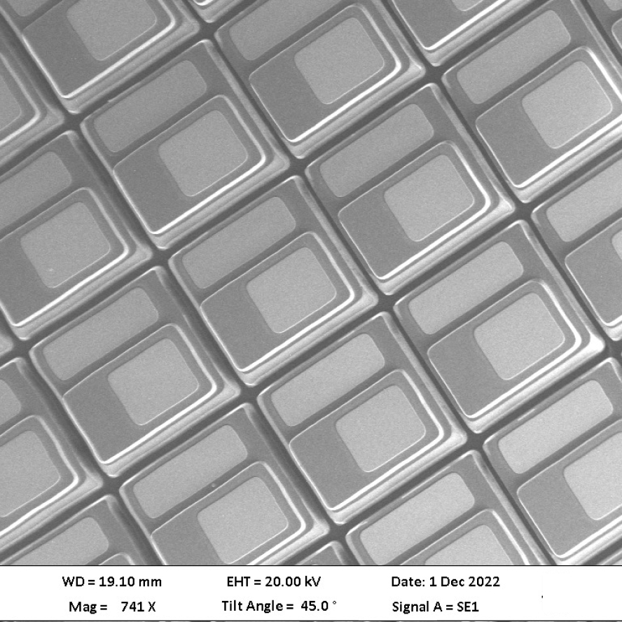 |
| Multilayered polyimide device | Arrayed LEDs |