Usable area
The design area for Poly MEMS is 10 mm x 10 mm but Science recommends designing chips to fit all critical elements within a 9.9 mm x 9.9 mm footprint.
 |
|---|
Place holes only where needed
The ANCHOR1, ANCHOR2, and POLY1_POLY2_VIA masks are designed to create holes between polysilicon layers, but should be filled in with a subsequent layer whenever possible. In the below example, the nitride layer has potential shorting issues and the polysilicon 0 layer has unintentional isolation issues.
 |  |
|---|---|
| The polysilicon 1 layer fails to cover all the holes. | Subsequent steps etch the nitride and polysilicon 0 layers away. |
Keep anchor masks distinct
The ANCHOR2 mask should be used to define holes from the polysilicon 2 layer to the polysilicon 0 or nitride layers. The same holes could be accomplished by combining geometries in the ANCHOR1 and POLY1_POLY2_VIA masks, but this would expose the polysilicon or nitride to overetching.
Place metal features on the polysilicon 2 layer
Depositing the metal layer is defined by two factors: surface availability and step conformality. The polysilicon 2 layer offers the best availability as it's oxide free—applying metal directly to the oxide 2 layer can work but leads to problems during release. The metal's internal resistance spikes dramatically over vertical steps due to the nature of the evaporative deposition process. Science recommends only depositing metal atop the polysilicon 2 layer.
Avoid long and thin features
In cases where the minimum design size is beneficial, isolated lines in the polysilicon layers should be kept to a 30 µm maximum—e.g. resonators. Thin features make lithography difficult when they get too long due to proximity effects and polysilicon reflectivity. Please discuss your design needs with Science if you feel that your design requires long, thin features.
Take care when designing breaches in the nitride layer
A few niche designs require breaching the nitride layer—e.g. the device needs to be grounded to the substrate layer. Our empirical data suggests the following approach to minimize contact resistance: 1) use the DIMPLE, POLY1_POLY2_VIA, and ANCHOR2 masks to breach the nitride; 2) remove the polysilicon 1 layer; 3) fill the hole with the polysilicon 2 layer. The DIMPLE mask feature should enclose the POLY1_POLY2_VIA feature by at least 7 µm, which should enclose the ANCHOR2 feature by at least 5 µm.
Creating double-thickness structures
The polysilicon 1 and polysilicon 2 layers can be stacked together to approximate a single 3.5 µm polysilicon layer. This is possible with the following steps: 1) draw a continuous sheet in POLY1; 2) draw a continuous POLY1_POLY2_VIA that encloses POLY1 by 5 µm; 3) draw the POLY2 structure over the POLY1 sheet with the desired pattern. Any features in the POLY2 mask will need to adhere to a minimum feature size of 3.5 µm to adjust to the increased layer thickness. If leads are drawn from the POLY1 mask structure, the POLY2 mask must enclose the POLY1_POLY2_VIA cuts by 3 µm.
 |
|---|
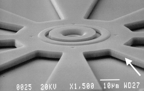
| Double thickness rotor with interface between polysilicon 1 & 2 layers highlighted. |
Be careful of galvanic attack
Galvanic attack of the polysilicon layers is possible during release if metal is present. Science cannot be held responsible for any effects on die yield caused by galvanic attack during release.
Conservative designs typically have higher yields
Defaulting to a minimum geometry for all lines, spaces, overlaps, and borders of 5.0 µm will lead to higher yield numbers—please note that design rules R and S will still require etch hole spacing to be a maximum of 30 µm.
Subdicing
Poly wafers can be subdiced with multiple cuts in each direction. The final length of the subdiced chips must be at least 2.5 mm or 5 mm if HF release or CO₂ drying is required. The dicing cuts will need to be drawn on the POLY0 mask with a line 150 µm wide.
General Release Instructions
All unreleased dice are shipped with a photoresist coating on the frontside to protect the structures from any dicing and shipping damage—this coating may be scratched on arrival. To remove it, soak the dice in acetone for 20-30 minutes and mildly agitate. The die should then be placed in isopropyl alcohol for several minutes and thoroughly rinsed in DI water.
To release your structures, use a bath of 49% HF at room temperature and release the die for 2.0–2.5 minutes with gentle agitation followed by 10 minutes in DI water and 5 minutes in isopropyl alcohol. Remove the die from the isopropyl alcohol and bake them for 10–15 minutes at approximately 110°C.
HF release and C0₂ drying
Science can perform a standard HF release designed to fully remove the sacrificial oxide from chips that have been designed with the proper etch hole spacing. Even after HF Release, device stiction is a common problem. Drying the chips after HF release by critical point drying in CO₂ will reduce stiction. The shortest allowable length of any side of a PolyMUMPs subdie is 5mm when HF release and/or CO₂ drying is required.
Software
Science uses Mentor Graphics to translate user files for the MEMS process. The below list details common issues Science is aware of with Mentor Graphics software though Science is not responsible for problems resulting from bugs listed here.
- CIF files require extended wire types or information may be lost. GDS files can use extended, butted, or rounded end wire types: rounded endings will be converted to truncated endings.
- Polygons with more than 1000 vertices cannot be processed by Mentor Graphics. These polygons should be broken into smaller polygons before submission.
- Manufacturing grids should be set to 0.1 µm or greater in L-Edit to reduce file size. Select Setup > Design > Grid to change the grid size.
- Illegal polygons caused by internal intersections cannot be processed by Mentor Graphics. Setting the points to be common or resizing the polygons slightly are the easiest solutions to this issue. This occurs most frequently in lettering and pictures translated to GDS file format.
 |  |
|---|---|
| Illegal shape | Legal shape |
General FAQs
What is the metal composition used in each MEMS process?
- Poly MEMS uses 20 nm chrome + 500 nm gold for the metal layer.
What is the gold purity of the gold used for the metal layers?
- The gold purity is 99.999%.
How is the metal deposited?
- The metal layer is deposited via evaporation with an electron-beam tool.
Is it possible to control the doping area of the polysilicon layers?
- No, it is not possible to control the doping area.