Creating wafers with the Poly MEMS process will result in a chip with eight layers: nitride, three polysilicon layers, metal, two sacrificial oxide layers, and a substrate.

| Thickness (µm) | Resistance (Ω/□) | Residual stress (MPa) | Purpose | |
|---|---|---|---|---|
| Nitride | 0.60 ± 0.07 | N/A | 90 ± 90 | This layer insulates the silicon layers from the substrate layer. |
| Polysilicon 0 | 0.50 ± 0.03 | 30 ± 15 | -25 ± 25 | This layer can be used for mechanical structures, resistor structures, and electrical routing. |
| Oxide 1 | 2.00 ± 0.25 | N/A | N/A | This layer is a sacrificial layer that supports the polysilicon layers during manufacturing but will ultimately be removed. |
| Polysilicon 1 | 2.00 ± 0.15 | 10.5 ± 9.5 | -10 ± 10 | This layer can be used for mechanical structures and resistor structures. |
| Oxide 2 | 0.75 ± 0.08 | N/A | N/A | This layer is a sacrificial layer that supports the polysilicon layers during manufacturing but will ultimately be removed. |
| Polysilicon 2 | 1.50 ± 0.10 | 20 ± 10 | -10 ± 10 | This layer can be used for mechanical structures and resistor structures. |
| Metal | 0.52 ± 0.06 | 0.06 ± 0.01 | 50 ± 50 | This layer is useful for bond pads, electrical routing, or optical mirrors. |
| Substrate | - | - | - | - |
Examples
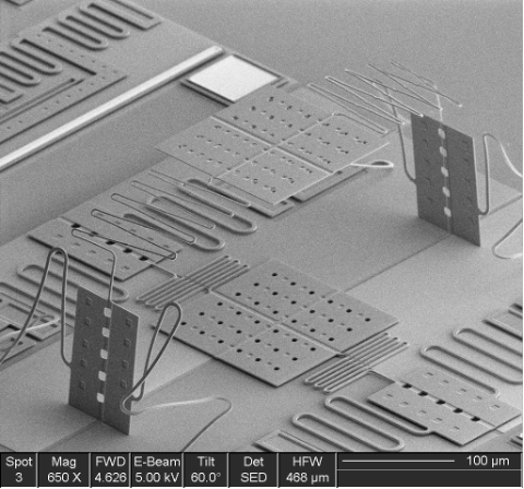 | 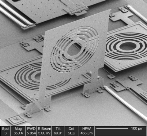 | 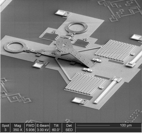 | 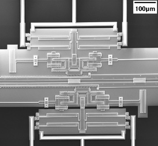 |
| Microthermal isolation platform | Fresnel-zone plate assembled by fluid flow | World's smallest catapult | Linear stepper motor |
Images courtesy of the School of Engineering Science at Simon Fraser University