Creating wafers with the TFE process will result in a chip with up to four layers: two polyimide layers and two metal layers.

| Layer name | Thickness (µm) | Purpose |
|---|---|---|
| Metal 1 | 0.24 | This layer is ideal for routing traces and defining electrode sites. |
| Top metal | 0.10 | This layer is ideal for remetallizing electrode sites and connection pads. |
| Polyimide 1 | 5 | This layer forms the base of the device. |
| Polyimide 2 | 5 | This layer insulates the routing traces. |
Examples
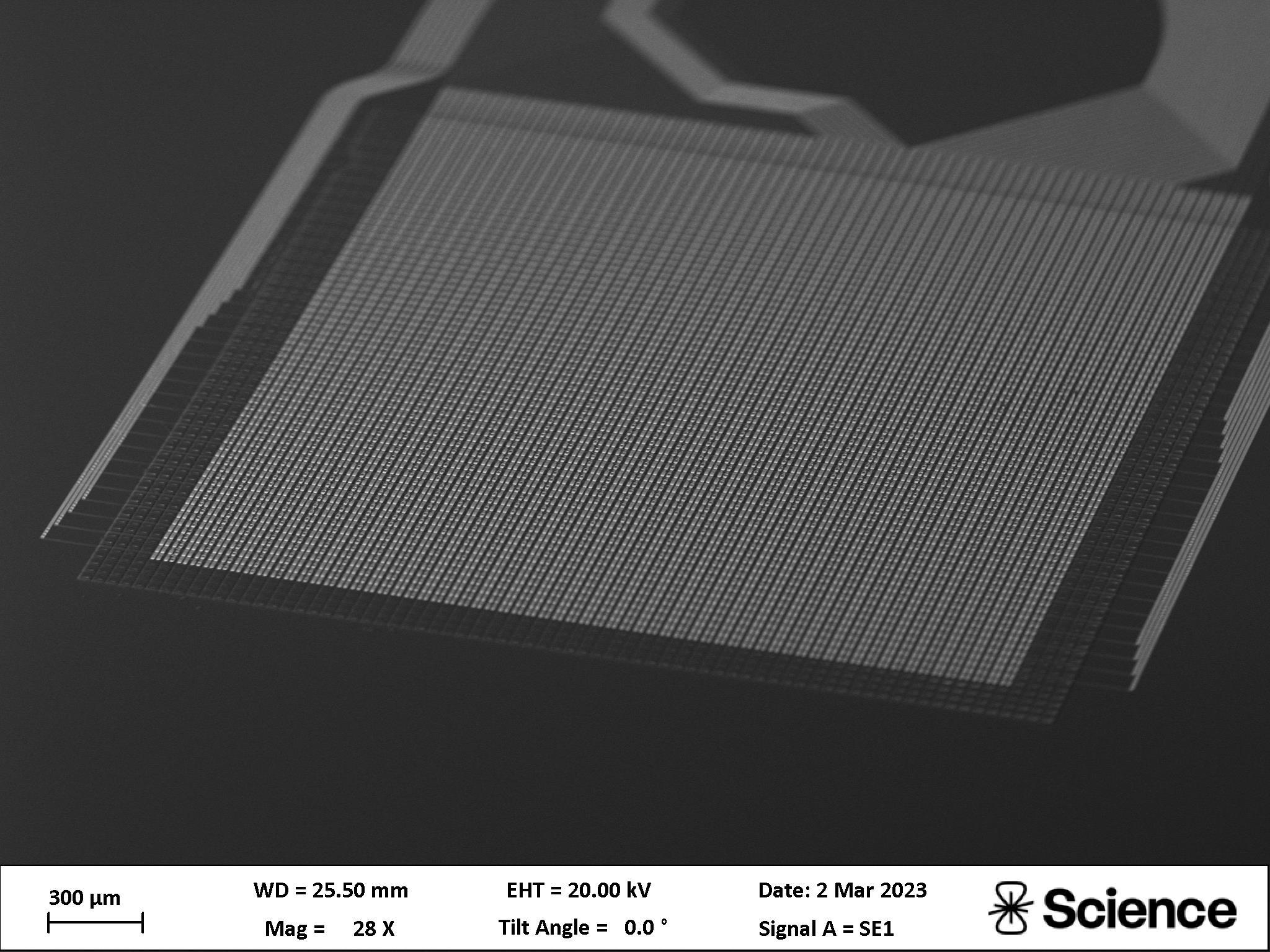 | 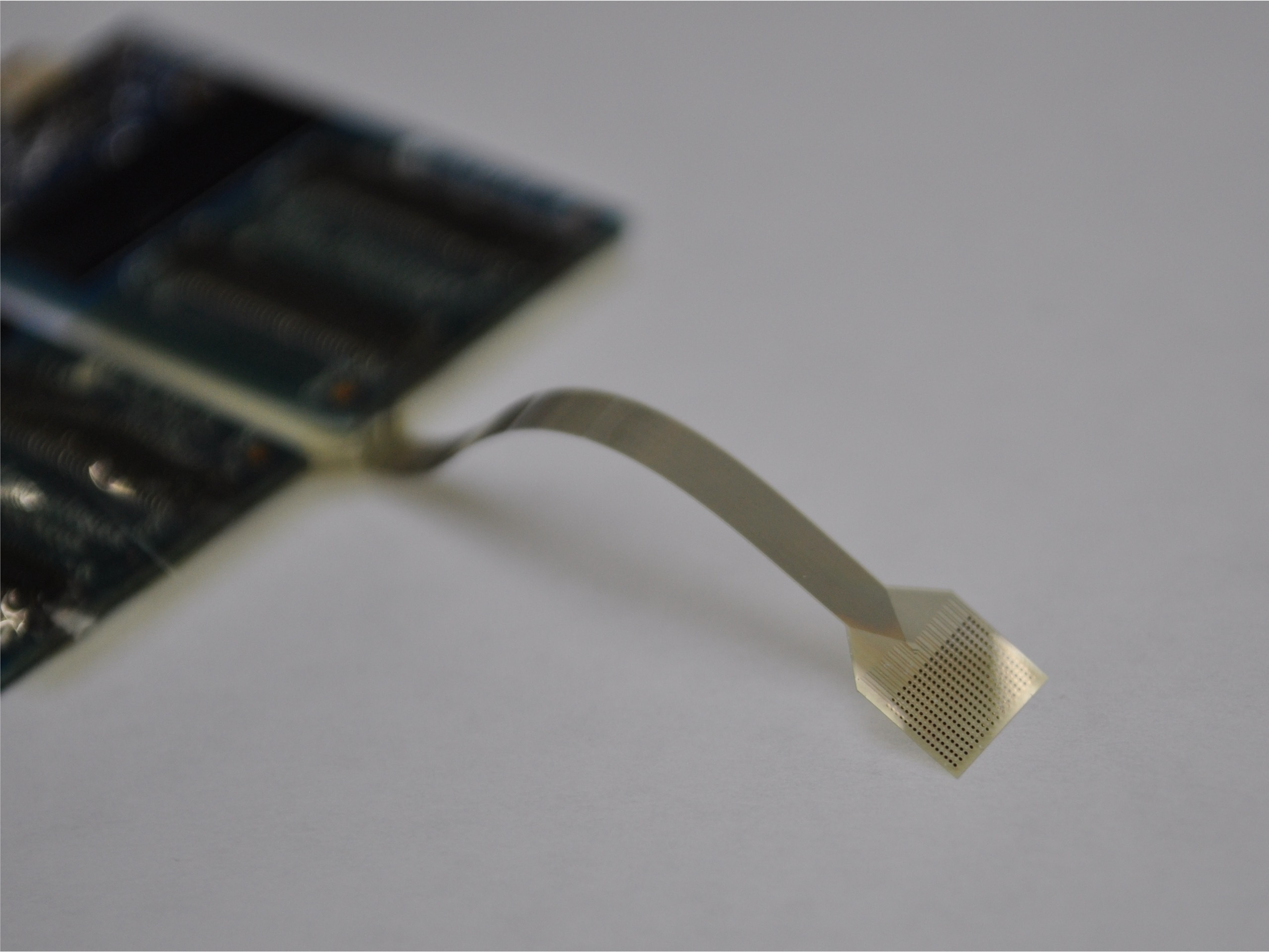 |
| Flexible neural electrode array | Multilayered polyimide device |