Creating wafers with the Piezo MEMS process will result in a chip with up to six layers: pad metal, piezoelectric film, pad oxide, silicon, buried oxide, and substrate.

| Thickness (µm) | Resistance (Ω/□) | Resistivity (Ω/cm) | Purpose | |
|---|---|---|---|---|
| Pad oxide | 0.202 ± 0.08 | N/A | N/A | This layer isolates the silicon from the piezoelectric film or pad metal layers. |
| Piezoelectric film | 0.5 | N/A | N/A | This layer can be used for piezoelectric sensors. The film uses aluminum nitride and has a strain coefficient between 3.4–6.5 (pC/N). |
| Pad metal | 1.02 | 0.055 ± 0.010 | N/A | This layer is perfect for precision alignment but is limited to areas not etched in the silicon. |
| Silicon | 10 ± 1 | 20 ± 5 | 5.5 ± 4.5 | This layer can be used for mechanical structures, resistor structures, and electrical routing. |
| Substrate | 400 ± 5 | N/A | 9.5 ± 0.5 | This layer can be etched with through-hole structures. |
| Buried oxide | 1.0 ± 0.05 | N/A | N/A | This layer insulates the silicon and substrate layers. |
Examples
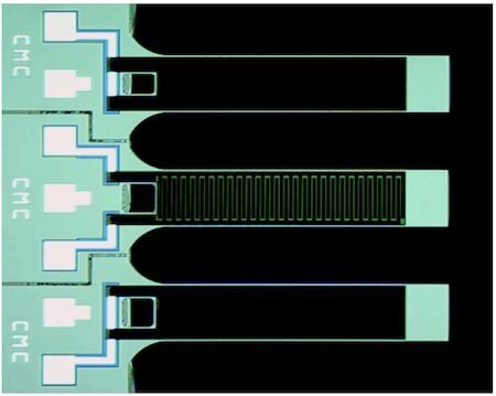 | 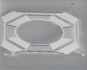 |
| Set of cantilevers with proof masses at tip | Bulk accelerometers |
| Image courtesy of Joan Pons-Nin et al. | Image courtesy of Gerfers et. al. |