Creating wafers with the SOI MEMS process will result in a chip with up to five layers: pad metal, silicon, substrate, buried oxide, and blanket metal.

| Thickness (µm) | Resistance (Ω/□) | Resistivity (Ω/cm) | Purpose | |
|---|---|---|---|---|
| Pad metal | 0.52 ± 0.10 | 0.055 ± 0.010 | N/A | This layer is perfect for precision alignment but is limited to areas not etched in the silicon and is not great for low loss optical mirrors. |
| Silicon | 25 ± 1 | 20 ± 5 | 5.5 ± 4.5 | This layer can be used for mechanical structures, resistor structures, and electrical routing. |
| Substrate | 400 ± 5 | N/A | 9.5 ± 0.5 | This layer can be etched with through-hole structures. |
| Buried oxide | 2.0 ± 0.1 | N/A | N/A | This layer insulates the silicon and substrate layers. |
| Blanket metal | 0.65 ± 0.07 | 0.045 ± 0.10 | N/A | This layer is useful for optical mirror surfaces and substrate contacts. |
Examples
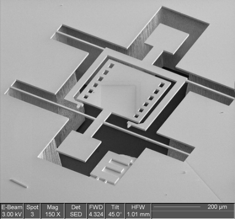 | 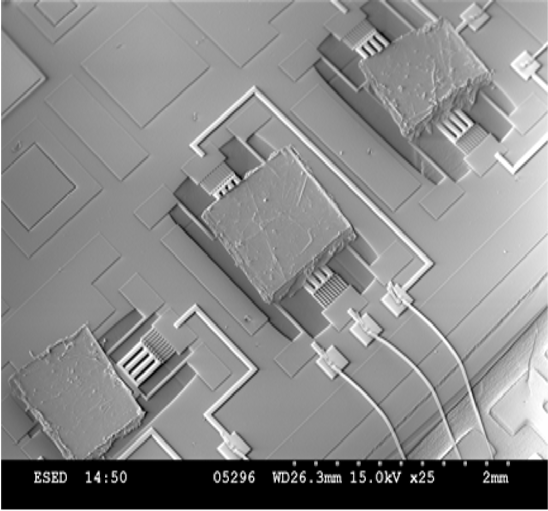 |
| Variable Optical Attenuator | Reflecting square attached to a silicon platform |
| Image courtesy of the School of Engineering Science at Simon Fraser University | Image courtesy of the Centre for Microsystems and Photonics at University of Strathclyde |