Usable area
The design area for SOI MEMS is 9 mm x 9 mm but Science recommends designing chips to fit all critical elements within a 8.5 mm x 8.5 mm footprint. The full size of the chip measures 11.15 mm x 11.15 mm.
 |
|---|
Silicon layer anchor and release
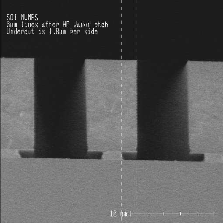
Structures in the silicon layer can be anchored to the substrate layer by ensuring they are at least 10 µm on each side and placing them 50 µm from the edge of the TRENCH mask. The size requirement is due to the undercut of the buried oxide layer during the HF vapor etch process. The undercut is typically about 1.9 µm but can be as large as 5.0 µm from each side.
Structures in the silicon layer can be released by etching the substrate layer out from under them.
| Desired effect | Distance requirement | Size requirement |
|---|---|---|
| Anchor a silicon structure to the substrate layer. | The SOI mask edge should be more than 50 µm from the TRENCH mask edge. | The SOI feature size should be greater than 10 µm if it's over a trench. |
| Release a silicon structure from the substrate layer. | The SOI feature should be fully enclosed by the TRENCH mask. | The SOI feature size should be less than 3.5 µm but up to 10 µm can be possible. |
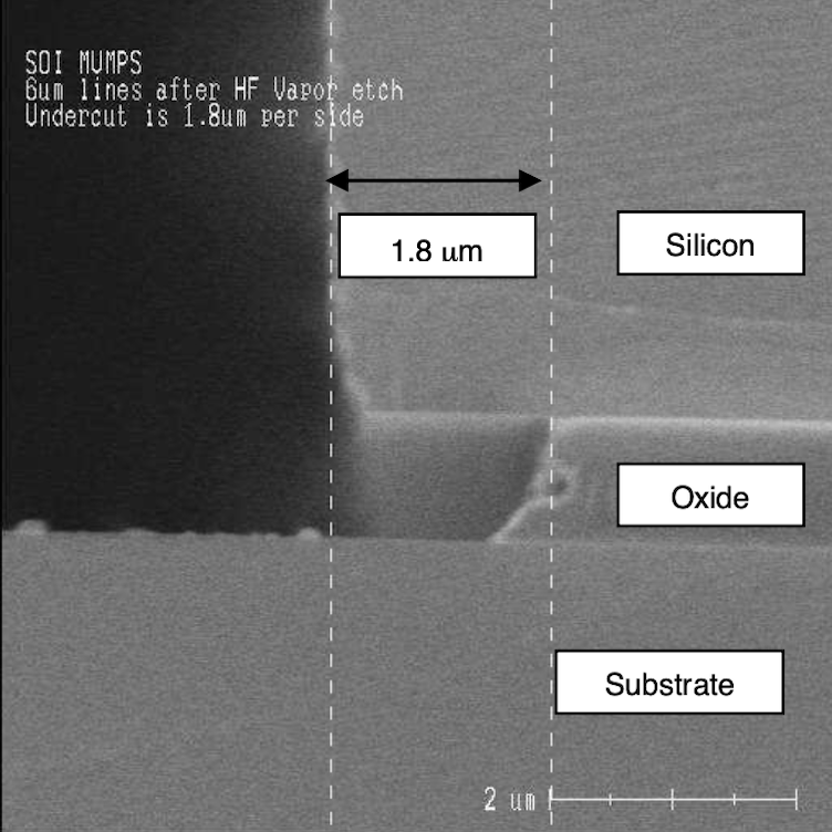
The buried oxide layer shown with a 1.8 µm undercut on each side:
 |  |
|---|
BLANKETMETAL mask constraints
The shadow mask used to apply the blanket metal layer cannot have internal geometries—i.e. no "doughnut" shapes. The BLANKETMETAL mask etches completely through the shadow mask so any internal geometries would fall away without supports.
 |  | |
| Allowable pattern | Unallowable pattern |
TRENCH mask constraints
Similar to the BLANKETMETAL constraints, internal geometries or "doughnut" shapes are not possible in the TRENCH mask. Even if they are suspended or supported from the silicon layer, internal geometries rarely survive the fabrication process. These "full thickness structures" are possible with the Piezo MEMS process.
 |  |  |
|---|---|---|
| Allowable pattern | Unallowable pattern | Unallowable pattern |
Subdicing
These wafers can be laser cut zero, one, or two times.
- Zero cuts yield one 11 mm x 11 mm die.
- One cut yields two 11 mm x 5.5 mm die.
- Two cuts yield four 5.5 mm x 5.5 mm die.
 |  |  |
|---|
Designed-in subdicing
If subdicing is desired, but not critical, SOI MEMS wafers can be designed for manual separation by designing the SOI and TRENCH masks to include perforating cuts.
- The SOI and TRENCH masks should both include dicing cuts 200 µm or wider that run from end to end.
- The TRENCH mask should not specify any other features within 500 µm of the dicing cuts.
 |
|---|
Anchor point reinforcement
Suspended structures in SOI MEMS are prone to cracking at the anchor points during the application of the protective material.
 |  |  |
| Filleted corners provide the best support. | Beveled corners provide medium support. | Right angled corners provide minimal support. |
Electrical isolation and routing
Electrical isolation between adjacent metal features is only possible if the silicon layer is divided. The surface doping of the silicon layer will connect adjacent features on the same surface. The undercutting of the buried oxide layer will prevent connectivity between adjacent silicon features.
 |  |
| These pad metal features are electrically isolated. | These pad metal features are electrically connected via the shared silicon layer. |
Dimples
Long, narrow beams in the silicon layer tend to stick together in the release process if they are placed close together. Adding dimples will reduce the stiction and ensure the beams will stay distinct.
 |  |
| The dimples on these silicon beams will lower the stiction. | These silicon beams will have a higher chance to stick together. |
Software
Science uses Mentor Graphics to translate user files for the MEMS process. The below list details common issues Science is aware of with Mentor Graphics software though Science is not responsible for problems resulting from bugs listed here.
- CIF files require extended wire types or information may be lost. GDS files can use extended, butted, or rounded end wire types: rounded endings will be converted to truncated endings.
- Polygons with more than 1000 vertices cannot be processed by Mentor Graphics. These polygons should be broken into smaller polygons before submission.
- Manufacturing grids should be set to 0.1 µm or greater in L-Edit to reduce file size. Select Setup > Design > Grid to change the grid size.
- Illegal polygons caused by internal intersections cannot be processed by Mentor Graphics. Setting the points to be common or resizing the polygons slightly are the easiest solutions to this issue. This occurs most frequently in lettering and pictures translated to GDS file format.
 |  |
|---|---|
| Illegal shape | Legal shape |
General FAQs
What is the metal composition used in each MEMS process?
- The pad metal layer uses 20 nm chrome + 500 nm gold.
- The blanket metal layer uses 50 nm chrome + 600 nm gold.
How is the metal deposited?
- The metal layer is deposited via evaporation with an electron-beam tool.
Is it possible to control the doping area of the polysilicon layers?
- No, it is not possible to control the doping area.