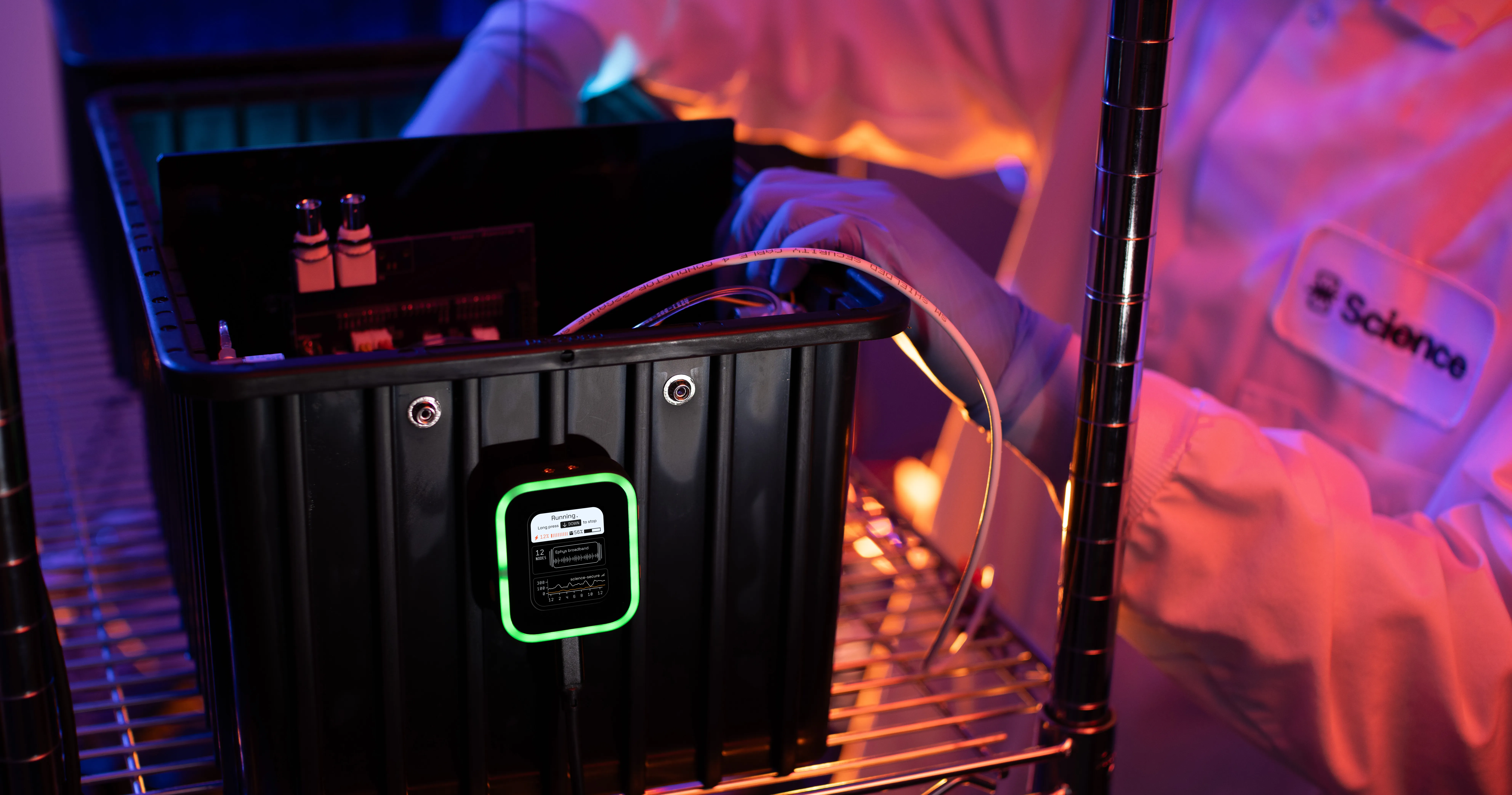

Science Foundry
Build on Science’s advanced MEMS capabilities for your own research or product development
Science Foundry is your fastest path from design to device
Iterate in weeks, not months, with no upfront investment required.
Sign up for free

Design with specialized wafer runs for complete control of the process or larger designs.
Join a scheduled run to gain the fastest turnaround times and user friendly documentation support.
Build a custom run with our diverse capabilities to achieve a high level of control, even at low quantities.
Over 80 tools spanning broad capabilities
LPCVD films
Important films, deposited on both sides of the substrate, provide excellent conformal coating, high breakdown and dielectric isolation
Low stress nitride
Low temperature oxide
LPCVD films
Important films, deposited on both sides of the substrate, provide excellent conformal coating, high breakdown and dielectric isolation
Low stress nitride
Low temperature oxide
Low stress polysilicon
Phosphosilicate glass (PSG)


Post processing
Tools designed for soft contact can place sensitive devices on substrates or packages or subdivide a chip.
Dicing
Pick and place
Lithography
Process by which a light-sensitive polymer, called a photoresist, is exposed and developed to form 3D relief images on the substrate.
Maskless alignment
Front to back alignment
Polymer films
Polymeric films are defined as thin continuous materials typically up to 200 μm (0.008 in.) thick.
Polyimide
Parlyene-C
Dry etching
Removal of plastic or other semiconductor material using plasma as opposed to chemical treatment.
DRIE
Plasma clean
Efficient, software-enabled custom process development
Metallization
Metal Deposition. After devices have been fabricated in the silicon substrate, connections must be made to link the circuits together.
Evaporation
Sputtering

Wafer bonding
Attachment of two or more substrates or wafers to one another through a range of physical and chemical processes
Si fusion
Glass-glass
Continuous investment in new tools and processes
Metrology
The science of measurement, embracing both experimental and theoretical determinations at any level of uncertainty.
SEM / FIB
Profilometry
Wet etching
Material removal process that uses liquid chemicals or etchants to remove materials from a wafer
KOH silicon etch
Wet oxide etch

Thermal processing
Temperature treatments for metal or silicon, customized to deliver specific material properties.
Silicon oxidation
Anneals

The fastest path from design to- biosensing
- quantum computing
- aerospace
- telecommunications
- neural engineering
Log into the Science Foundry to see our available technologies, shuttle runs, and to place orders
Log in