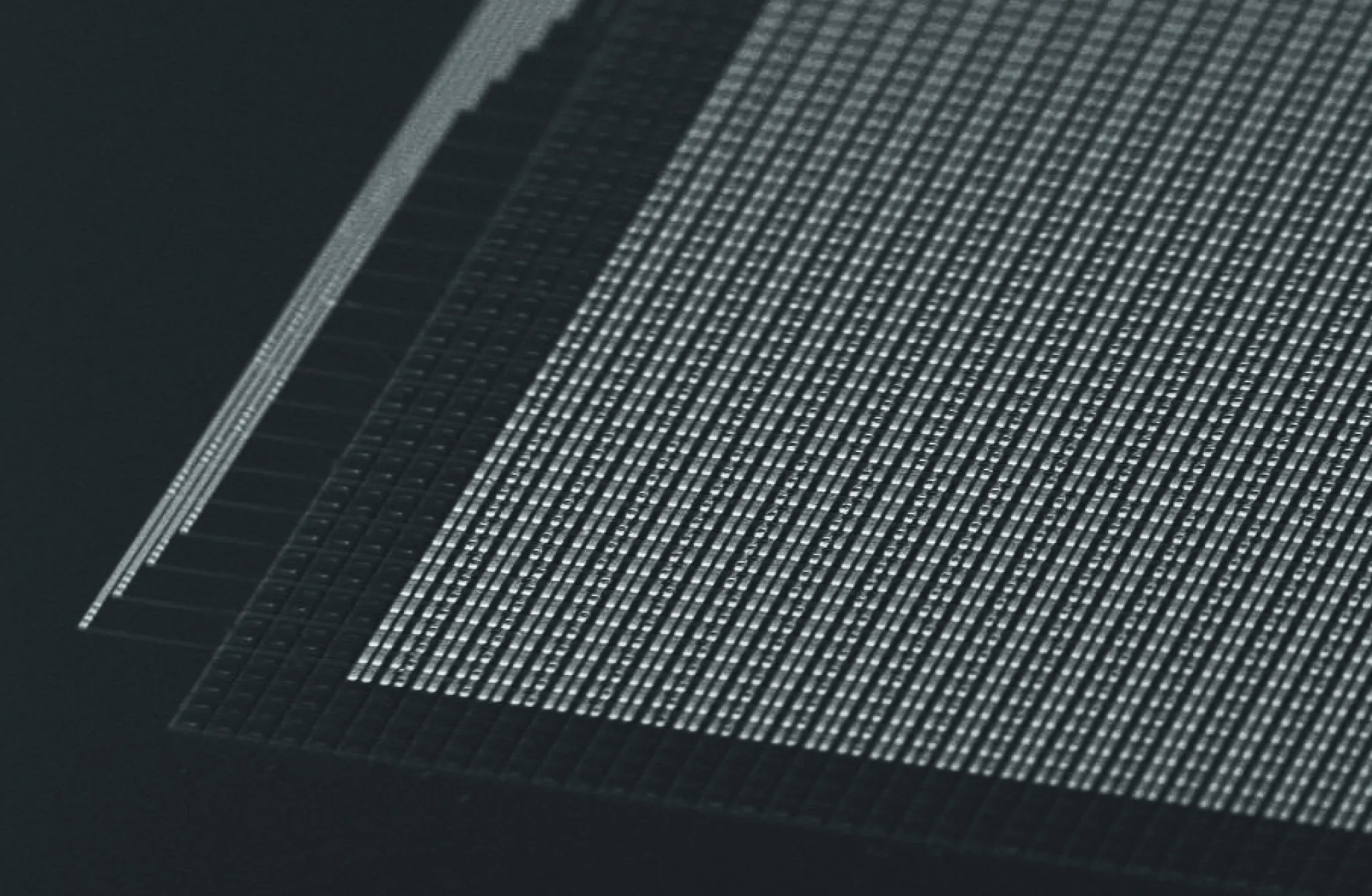
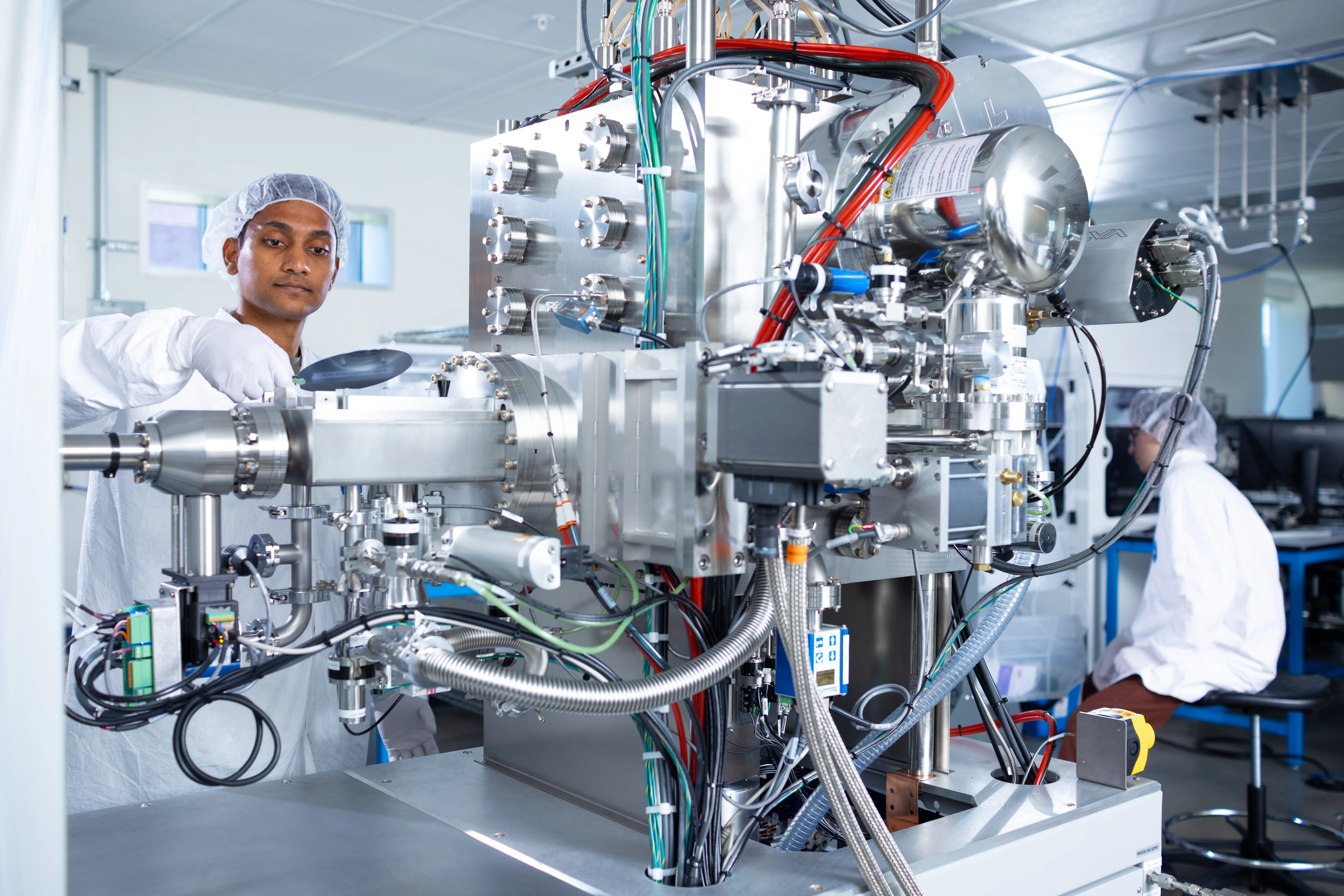
Decades of experience and extensive process documentation makes MEMS design straightforward
Our Standard Technologies platform is a set of well-characterized MEMS fabrication processes that provide a proven platform for building innovative new devices. We offer regularly scheduled Multi-Project Wafer (MPW) runs of our SOI, Poly, and Piezo Technologies, as well as offering dedicated Thin Film Electronics wafer runs and custom process development.
Scheduled Standard Technology runs deliver our fastest turnaround times and most thorough characterization, while our dedicated wafer runs give you complete control of the process, larger designs, and a direct path to productization.

Learn more about our Standard Technologies
Silicon on Insulator
Four masks, a SOI wafer, and two metal layers provide a structured approach to silicon designs.
SOI documentationPolysilicon
Eight masks, three polysilicon layers, and one metal layer can be modified for the highest degree of customization.
Poly documentationPiezoelectric
Five masks, a SOI wafer, and distinct metal and piezoelectric layers offer an efficient ecosystem for piezo designs.
Piezo documentationThin Film Electronics
Two or three polyimide layers alongside a range of masks and metals create an ideal setup for electrode and LED designs
TFE documentation
