Custom Process Development

Partner with Science Corporation to scale your prototype to production

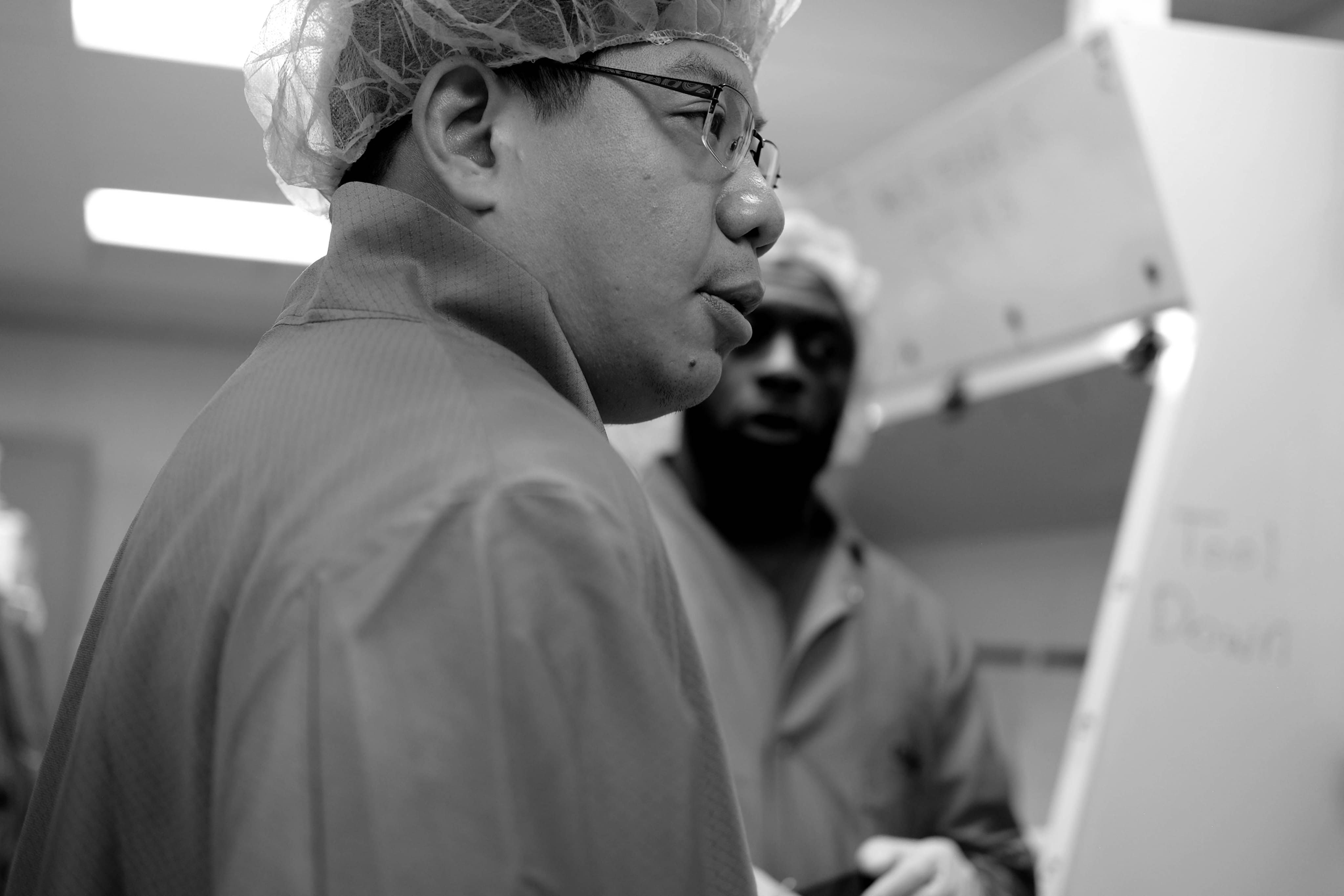
Science Foundry works with clients across diverse industries, guiding projects beyond the scope of our Standard Technologies from concept to full-scale production.

Our engineers bring specialized expertise and hands-on support to every stage of development, complementing the wide range of advanced tools and capabilities available at Science Foundry. With deep knowledge in material and layer integration, we can create bespoke solutions utilizing non-standard materials rarely available in CMOS foundries—such as gold, noble metals, polymers, piezoelectrics, glass, quartz, III-N semiconductors, and more.

Start a conversation
Graphic showing a transition between the conceptual, line art of an electrode and the final, realized product.

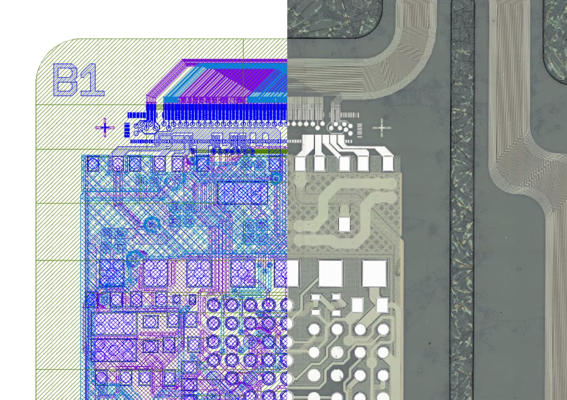
Production Process Overview
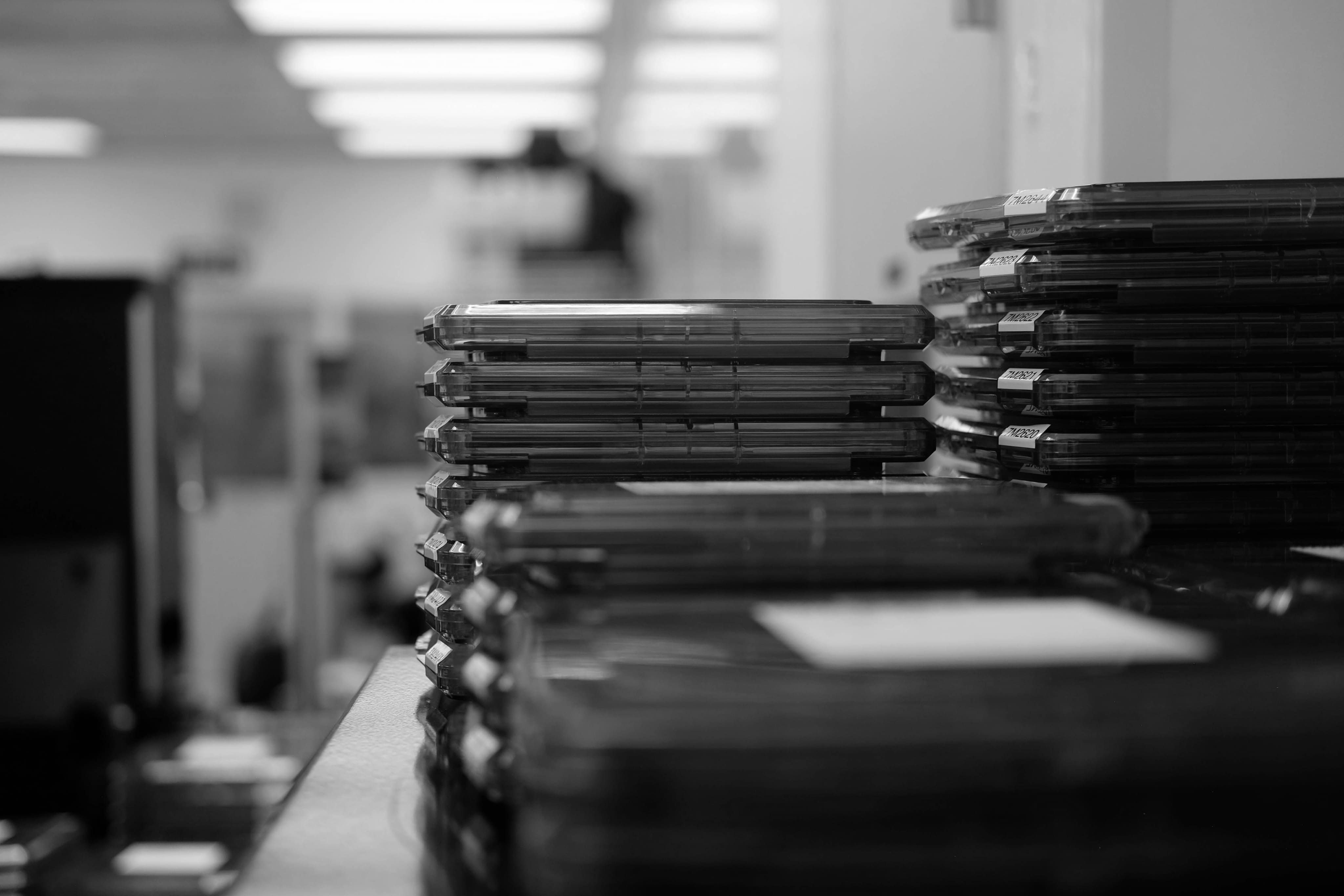
Production Volume

Chart showing how production volume increases. Chart showing how production volume increases.
  1. Feasibility Review

    Review prototype specifications and process flow to determine feasibility in our fab.

  2. Development Runs

    We collect data, identify issues, and adjust tools as we repeat the production process at least three times.

  3. Pre-Production

    Process validation at a large scale and any final adjustments before full-scale production.

  4. Production

    Production of devices at desired volume and schedule based on agreed specifications. 10s to 1000s of wafers.

More than 80 tools spanning broad capabilities

LPCVD films

  • Low stress nitride

  • Low temperature oxide

  • Low stress polysilicon

  • Phosphosilicate glass (PSG)

Clean room operator inspecting the inside of a machine. A microscope with four objectives is prepared for use.

Post processing

  • Dicing

  • HF liquid release

  • Critical CO2 drying

Lithography

  • Contact lithography

    Negative/positive resists, SU-8 and polyimide processing

  • Projection lithography

    Negative/positive resists, SU-8 and polyimide processing

  • Backside alignment

    Negative/positive resists, SU-8 and polyimide processing

  • Polymer films

    • Polyimide

    • Parylene-C

    • Backside alignment

    Dry etching

    • DRIE

      Si

    • RIE

      Poly-Si, SiO2, SiN, Polyimide, Parylene, and more

    • Plasma cleaning

      Plasma ashing is also possible

    Currently tooled for 6 inch wafer size

    Metallization

    • Evaporation

      Au, Cu, Ti, Cr, Pt, Ni, Al

    • Sputtering

      Cr, Au, Ti, TiW, Cu

    A stack of polished wafers are stashed vertically in organized dividers.

    Wafer bonding

    • Fusion

    • Glass-glass

    • Silicon-glass

    • Eutectic

    • Anodic

    Efficient, software-enabled custom process development

    Metrology

    • SEM

    • Profilometry

    • Infrared inspection

    • Interferometry

    • Film analysis

      Film stress, thickness, or resistivity

    Wet Etching

    • Si etching

      KOH

    • Wet oxide etching

      BOE, HF, HCl

    • Wet metal etching

      Au, Cr

    • Immersion cleaning

      SC1, HCL

    • Spray & solvent cleaning

    Stacks of finished product sit in neat packages.

    Thermal processing

    • Silicon oxidation

    • Annealing

    Two operators discuss technique outside the clean room.