LPCVD films
Important films, deposited on both sides of the substrate, provide excellent conformal coating, high breakdown and dielectric isolation.
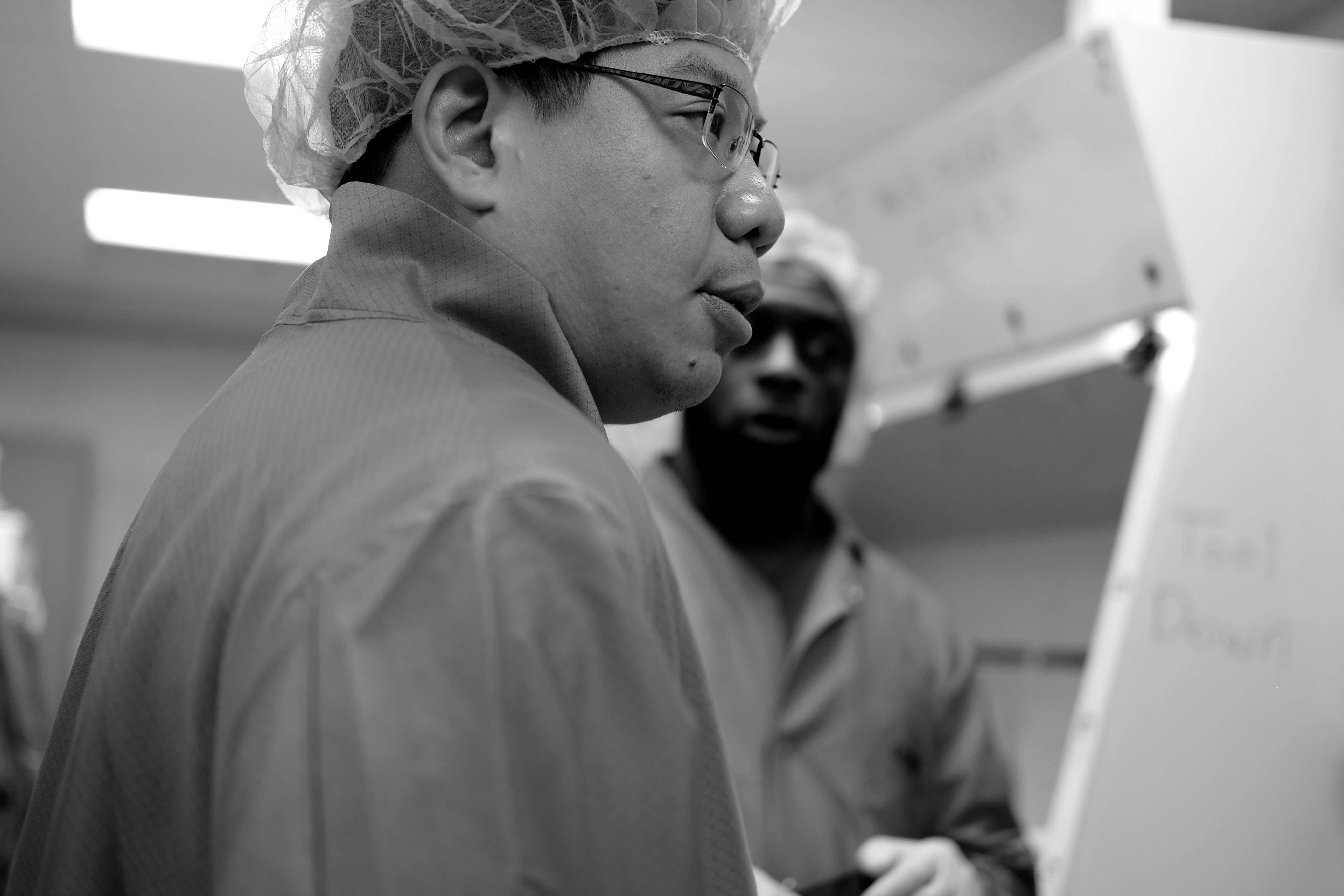
Have a project beyond our Standard Technologies? No problem. Science Foundry works closely with customers across a wide range of industries from conceptualization to volume production to achieve the best possible results for the most advanced possible products.
Our engineers bring expertise and dedicated support to the development process to complement the wide variety of tools and capabilities available at Science Foundry. Our bespoke solutions utilize the extensive material and layer integration knowledge we've built over years including non-standard materials not typically available in CMOS foundries like gold and other noble metals, polymers, piezoelectrics, glass, quartz, III-N, and more.
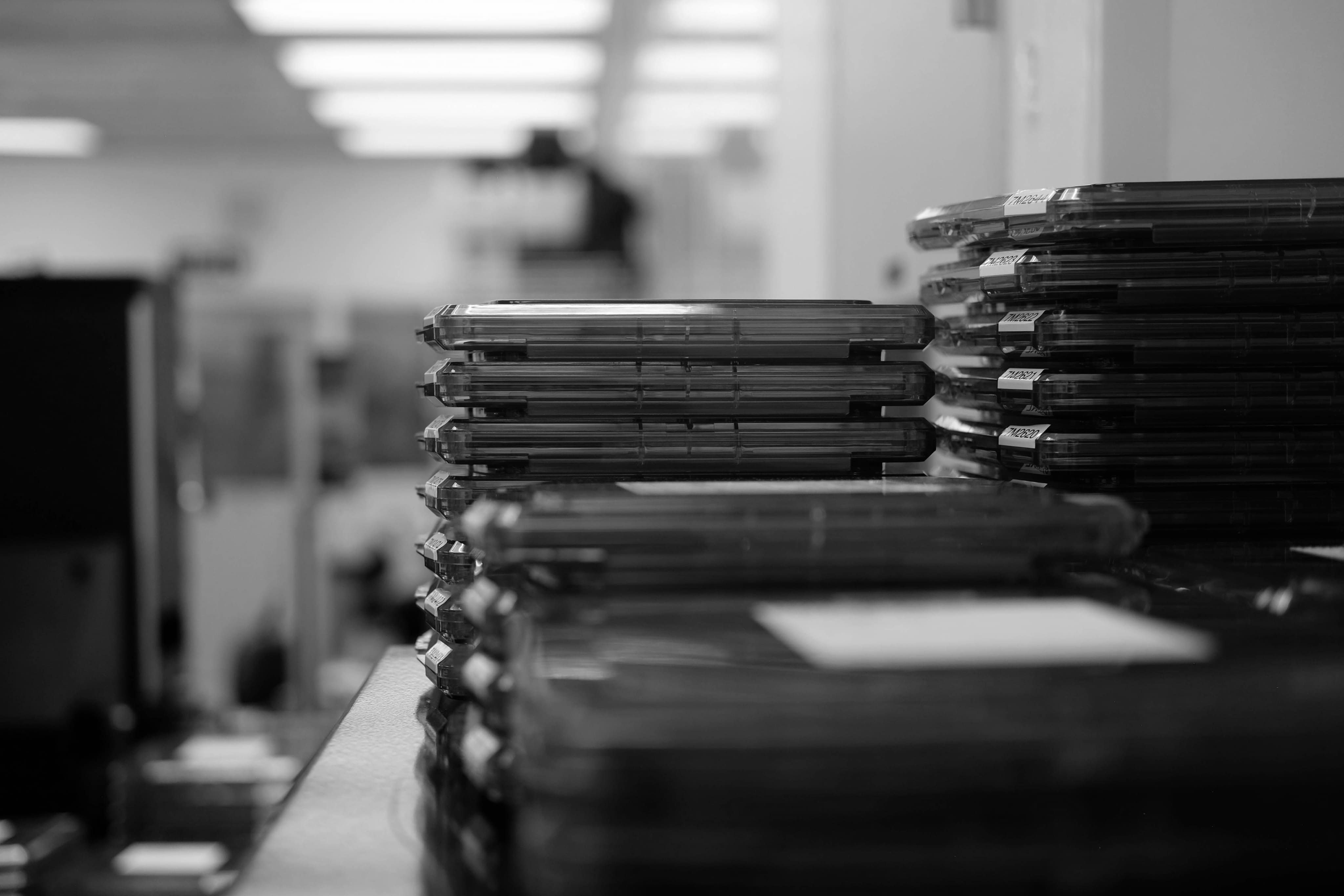
Our Capabilities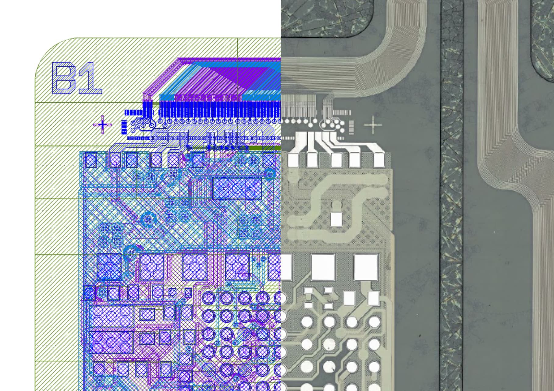


The customer presents their prototype and specifications to discuss process requirements.
We collect data, identify issues, and adjust tools as we repeat the production process at least three times.
Process validation at a large scale and any final adjustments before full-scale production.
Delivery of customer's device at desired volume and schedule.
LPCVD films
Important films, deposited on both sides of the substrate, provide excellent conformal coating, high breakdown and dielectric isolation.
Post processing
Tools designed for soft contact can place sensitive devices on substrates or packages or subdivide a chip.
Lithography
Process by which a light-sensitive polymer, called a photoresist, is exposed and developed to form 3D relief images on the substrate.
Polymer films
Polymeric films are defined as thin continuous materials typically up to 200 μm (0.008 in.) thick.
Dry etching
Removal of plastic or other semiconductor material using plasma as opposed to chemical treatment.
Metallization
Metal Deposition. After devices have been fabricated in the silicon substrate, connections must be made to link the circuits together.

Wafer bonding
Attachment of two or more substrates or wafers to one another through a range of physical and chemical processes.
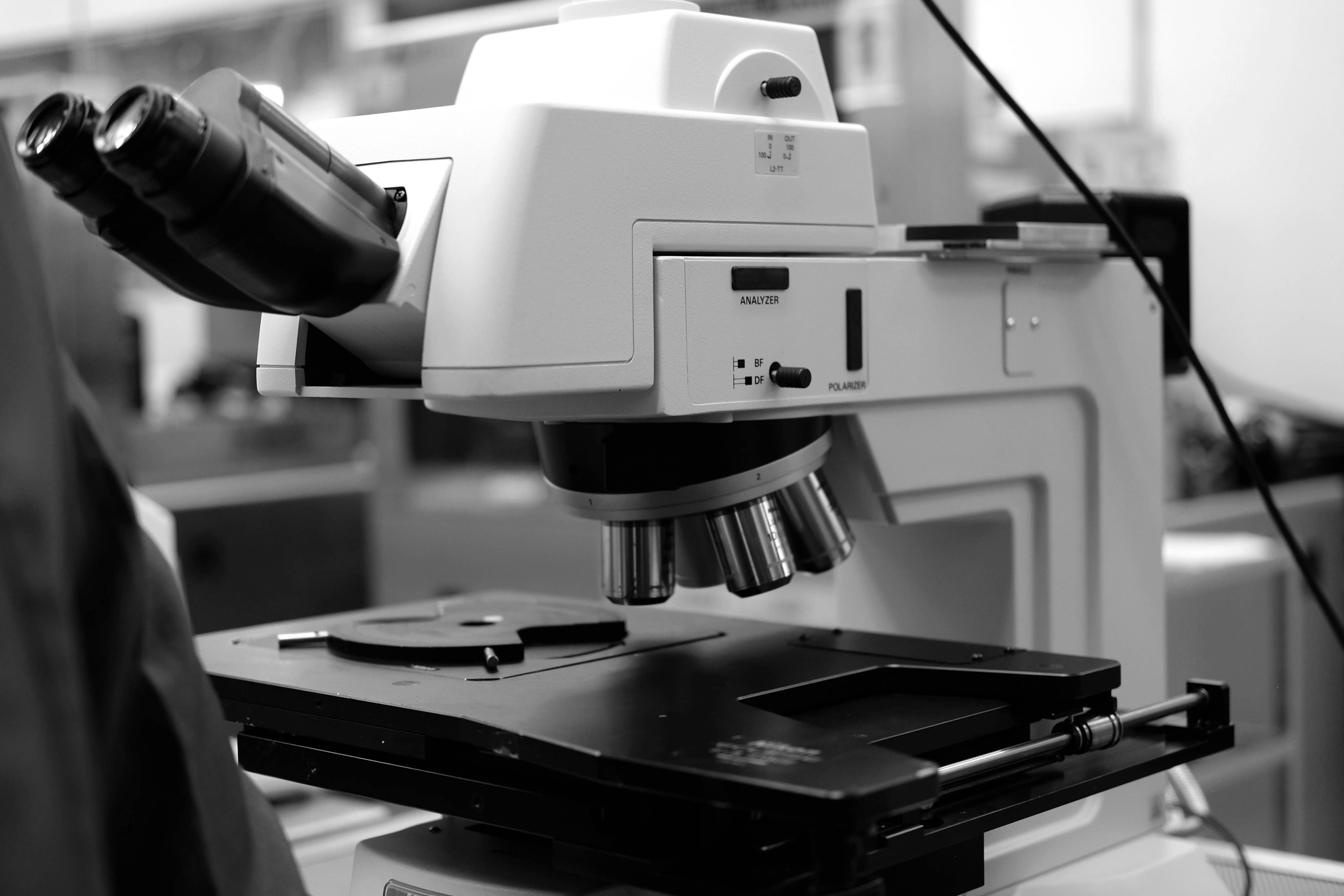
Metrology
The science of measurement, embracing both experimental and theoretical determinations at any level of uncertainty.
Wet Etching
Material removal process that uses liquid chemicals or etchants to remove materials from a wafer.
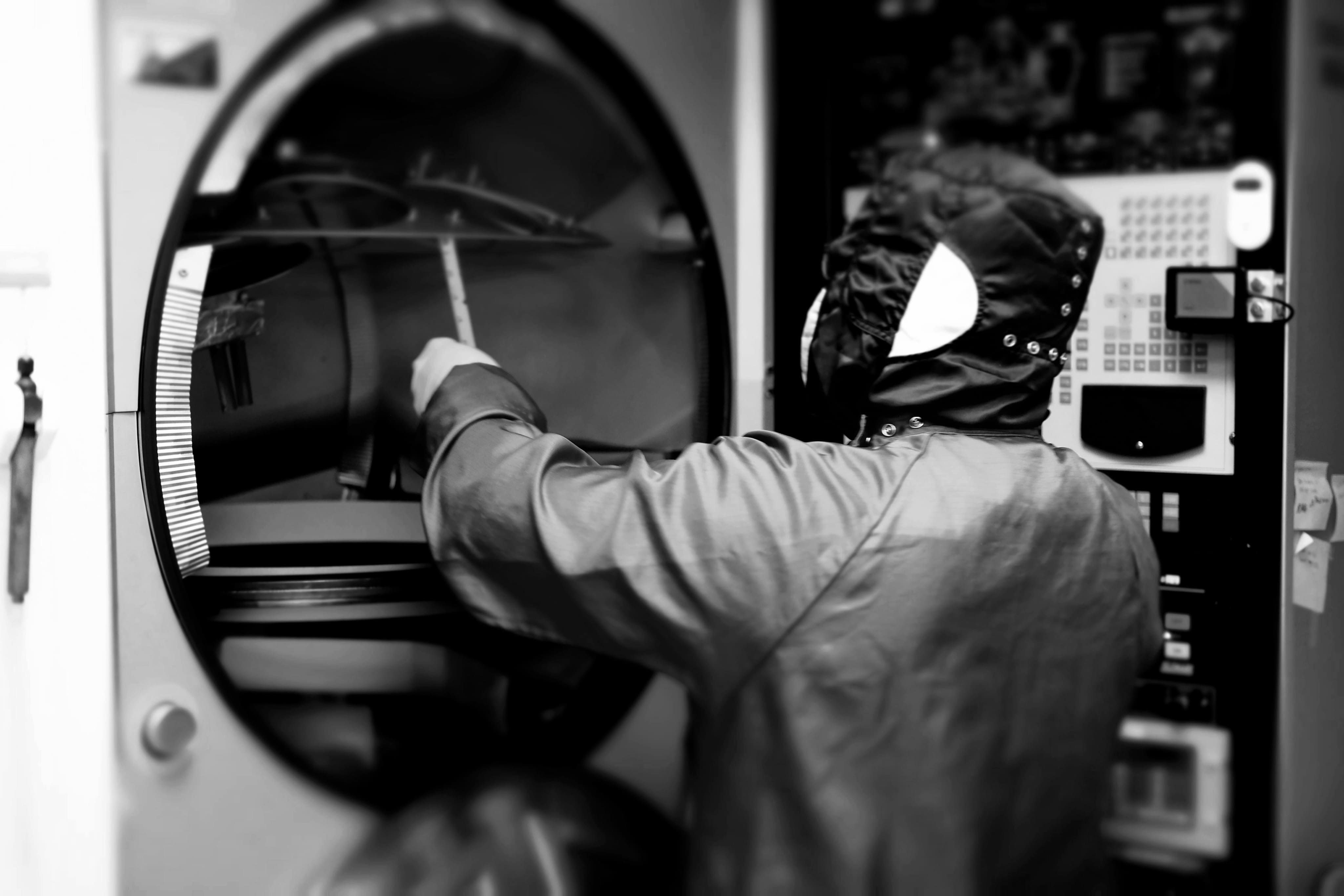
Thermal processing
Temperature treatments for metal or silicon, customized to deliver specific material properties.